About MOS
Metal-oxide-semiconductors (MOS) are very important in electronics. They are current switches at the level of electrical signals. MOS is represented as a sandwich from several layers of isolating material. The base of the “sandwich” is a thin round silicon wafer. Then goes a layer of the isolation layer - silicon dioxide ($SiO_2$)
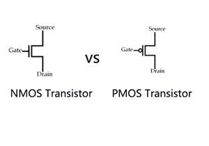
There are two types of MOS: NMOS and PMOS.
NMOS (on the left side of the image) is a form of MOS-transistor that contain semiconductor material of n-type in the channel. If the gate voltage is applied, the current flows.
PMOS (on the right side of the image) is a form of MOS-transistor that contain semiconductor material of p-type in the channel. It conducts in response to a negative gate voltage (less than threshold).
How it works
You must remember that in p-type semiconductor the current flows via positive charged particles(holes) and in n-type semiconductor via negative charged particles.
Let’s take NMOS as an example. When there is no voltage on the gate, NMOS is like a diode. When there voltage appears positive charged particles repell from gate and negative charged particles pull there. It makes a ‘bridge’ between source and drain where current can flow.
The same situation is with PMOS. When positive voltage is applied to gate, there is no ‘bridge’, but negative voltage opens the ‘bridge’ and current starts to flow.
NMOS
- Substrate and alloying
-
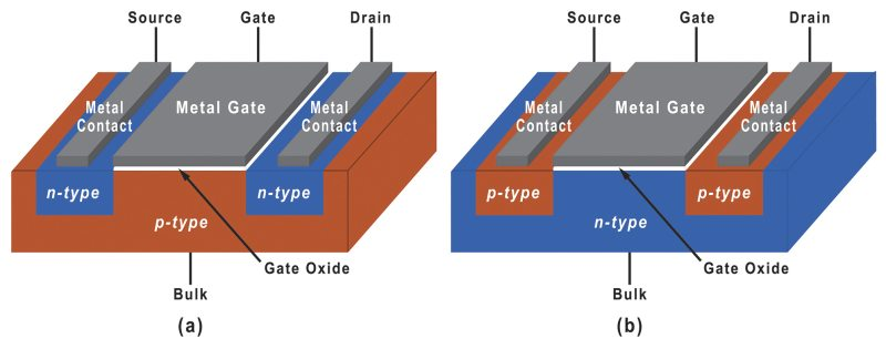
The substrate: P-type (positively doped).
-
Source and drain: N-type (negative alloying impurities).
If no voltage is applied to the gate, it will remain in the OFF state, and there will be no conductive path between the source and drain. But if a positive voltage is applied to the gate terminal, then electrons from the source and drain regions are attracted to the channel. This creates an n-type inversion layer that allows current to flow from drain to source. The current is a function of the gate-source voltage $V_{GS}$ and the drain-source voltage $V_{DS}$.
- Charge carrier and current
- Carrier: Electrons (high mobility)
- Active mode: drain to source when switched on.
- Shutter control outputs and frame input voltage
- Turns on when: The gate voltage is positive relative to the source ($V_{GS}$ > $V_{th}$)
- Threshold voltage ($V_{th}$): Lower than PMOS.
NMOS transistors use electrons as charge carriers, which have more mobility than holes (used by PMOS transistors). Higher electron mobility allows for faster switching speeds, making NMOS transistors ideal for high-speed digital circuits. However, NMOS transistors also suffer from static energy consumption, as they also pass current when turned off.
- Productivity and efficiency
- Switching speed: faster due to the mobility of the electrons.
- Resistance: Low, which ensures higher efficiency and lower power loss.
- Placement in CMOS circuits
- Used in: Grounding networks (earth anchoring).
PMOS
- Substrate and alloying
- Substrate: n-type (negatively doped).
- The substrate: P-type (positively doped).
In the absence of gate voltage, the transistor remains in the off state without a conductive channel. But when a negative voltage is applied to the gate, it pushes electrons away from the channel area, creating a p-type inversion layer. This allows the holes to migrate from the source to the drain, ensuring the flow of current. The PMOS transistor will remain switched on as long as the gate voltage is lower than the source voltage relative to the threshold voltage ($V_{th}$).
- Charge carriers and current
- Electricity Transportation: Holes (low mobility)
- Working direction: from source to drain
- Gate control and threshold voltage
- Turns on when: The gate voltage is negative than the source voltage ($V_{GS}$ < $V_{th}$).
- Threshold voltage ($V_{th}$): greater than NMOS.
- Productivity and efficiency
- Polarization switching rate: low due to hole mobility
- Resistance: more, resulting in more power dissipation.
- Placement in CMOS circuits
- Used in: Pull-up mesh ($V_{dd}$ connection)